Tel:+86-0572-2926332 / 2926337
E-mail:[email protected]
 English
 简体中文
简体中文Silicon Nitride in Semiconductors
2025.09.23
Silicon nitride () is a material that has played a pivotal role in the advancement of semiconductor technology. While often overshadowed by silicon dioxide (), its unique properties make it indispensable for a variety of applications, from passive device components to active transistor elements.
The Unique Properties of Silicon Nitride
Silicon nitride possesses a combination of properties that make it a superior choice for specific semiconductor applications:
-
High Dielectric Constant (): Compared to (with a of around 3.9), has a higher dielectric constant (typically ranging from 7.5 to 8). This property allows for the storage of more charge in a given area, which is crucial for reducing the size of capacitors and memory cells. In dynamic random-access memory (DRAM), for instance, a higher material like helps maintain sufficient capacitance as cell dimensions shrink, preventing data loss.
-
Excellent Diffusion Barrier: One of the most critical functions of in semiconductor manufacturing is its ability to act as a highly effective barrier against the diffusion of atoms, particularly water molecules and alkali ions like sodium. This property makes it an ideal material for passivation layers and encapsulation films, protecting the delicate active areas of a chip from environmental contamination that could degrade device performance and reliability.
-
High Mechanical Hardness: The material's inherent hardness and mechanical strength make it suitable for use as a hard mask in lithography and etching processes. Unlike softer materials, can withstand aggressive plasma etching, allowing for the precise transfer of intricate patterns onto underlying layers with minimal erosion. This is particularly important for fabricating high-aspect-ratio structures.
-
Low Thermal Expansion Coefficient: The thermal expansion coefficient of is relatively low and closely matches that of silicon. This similarity minimizes mechanical stress on the device during thermal cycles, such as those encountered during processing steps like annealing and deposition. Reduced stress helps prevent cracking and delamination, improving overall device yield and longevity.
Key Applications in Semiconductor Devices
Silicon nitride is employed in a variety of critical roles within a semiconductor chip:
-
Dielectric Spacer: In the fabrication of FinFETs and other advanced transistor architectures, is used as a spacer material. These spacers electrically isolate the gate from the source and drain terminals, a vital function for preventing short circuits and controlling the channel length.
-
Gate Dielectric: While remains the standard for traditional MOS transistors, can be used in gate dielectric stacks to achieve higher capacitance and lower leakage currents. This is especially relevant in non-volatile memory technologies, such as floating-gate flash memory, where it can serve as a charge-trapping layer or as part of a multi-layer gate dielectric stack (e.g., stack: //).
-
Passivation and Encapsulation: As a final protective layer, a film of can be deposited over the entire chip surface. This passivation layer shields the integrated circuits from moisture, chemicals, and mechanical damage, significantly enhancing the long-term reliability of the device.
-
Interlayer Dielectric (ILD): In some applications, is used in inter-metal dielectric layers to separate different conductive interconnects. Its high density and barrier properties prevent the diffusion of metal atoms (like copper) into the surrounding dielectric, which is a common failure mechanism in advanced interconnects.
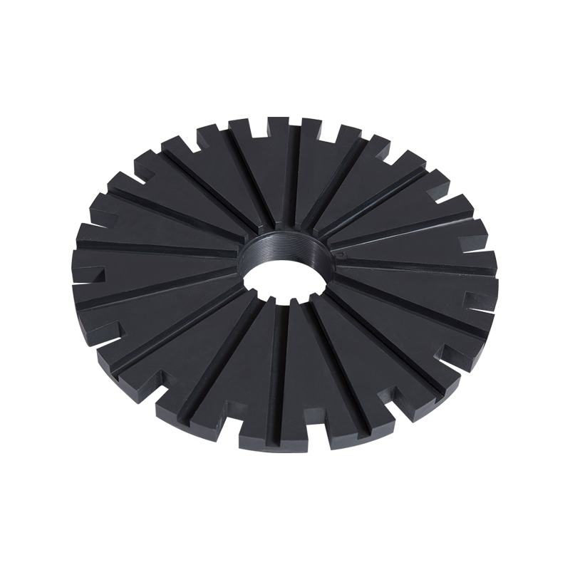
The Role of Silicon Nitride Ceramic
It is also worth noting the broader applications of silicon nitride beyond thin-film deposition on wafers. High-purity Silicon Nitride Ceramic is used to create components for semiconductor manufacturing equipment itself. Its exceptional hardness, thermal shock resistance, and chemical inertness make it ideal for parts like wafer handling tools, furnace tubes, and various fixtures that operate in harsh, high-temperature environments. This dual role—as a material on the chip and in the machinery that makes the chip—highlights its importance to the entire industry.
In conclusion, silicon nitride's unique combination of electrical, mechanical, and chemical properties has solidified its place as a critical material in modern semiconductor fabrication. Its ability to serve as an effective diffusion barrier, a high- dielectric, and a mechanically robust hard mask ensures its continued relevance as chip technology progresses to ever smaller and more complex scales.
Hot Products


Contact Us for Quotes and Prices!
Just let us know what you want, and we will get in touch with you as soon as possible!
We will continue to develop and produce more advanced ceramic materials for the aluminum processing industry.
Scan the Mobile QR code
Contact
 +86-18501518842 / +86-13587222672
 +86-0572-2926332 / 2926337
 +86-0572-2926335
 [email protected] / [email protected] / [email protected]
 No.11 Building, South Taihu High-tech Intelligent Manufacturing Industrial Park, Wuxing District, Huzhou City, Zhejiang, China
Copyright© 2024 Zhejiang Shangguijuli Special Material Technology Co., Ltd. All Rights Reserved. Ceramic Material Supplier
